Edge computing has made artificial intelligence nearer to the sources of data, which include sensors, mobile devices, cameras, and connected appliances. Data processing devices required in this dynamic environment need to process the data quickly and accurately, in many cases requiring real-time, with minimal or no dependence on cloud infrastructure. This transformation is transforming the PCB design, particularly, as the requirement to offer solutions that balance power efficiency requirements and computing performance increases. This dual requirement is the cause of a unique set of opportunities and trouble as far as businesses in a wide range of industries, including automotive, consumer electronics, medical technology, industrial automation, etc are concerned in terms of PCB design service and PCB layout service provided.
Considerations for Thermal Management
Even on Edge devices, AI processing can produce a lot of heat. Device performance might quickly deteriorate without proper heat management, which could result in failure. Proper PCB design must be considered to achieve effective distribution of heat especially on small layouts where there is hardly any airflow.
To guarantee that appropriate dissipation pathways are incorporated into the layout, the thermal profile of every component is examined throughout the design stage. Thermal reliability is considerably more important for equipment used in hostile settings, such as outdoor or industrial settings.
Thermal simulations are frequently performed by expert PCB layout service providers to assess heat flow generally. By improving board size, location, and copper distribution, these insights assist in maintaining crucial components within operating temperature ranges. Edge AI devices can perform complex algorithms on the edge without throttling or overheating if the thermal design is appropriate.
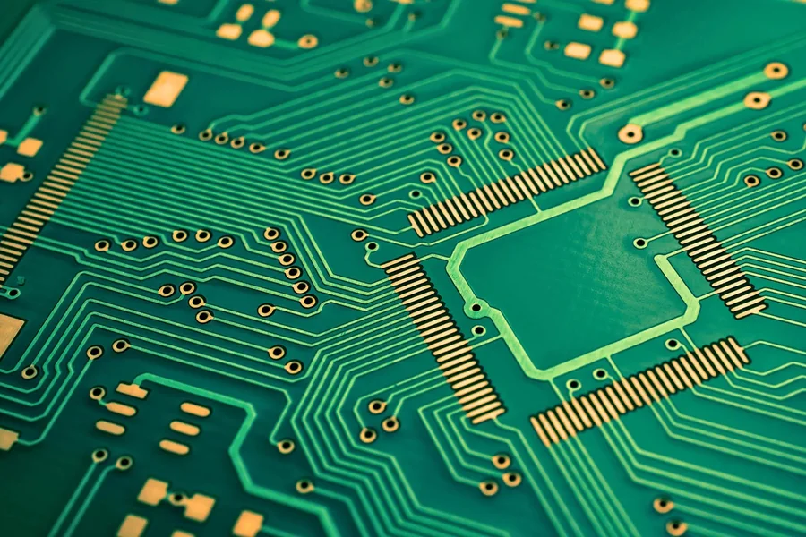
Compliance with EMI/EMC and Signal Integrity
Signal integrity is a must for Edge AI devices that depend on fast connectivity, whether via wireless modules, sensors, or processing units. This could disrupt the operations of the whole device through interference, delay, and loss of data. PCB design that will meet the high-frequency performance requires appropriately terminated PCBs that are designed with controlled impedance and a good grasp of transmission line characteristics.
Sensitive signals must be routed but ground reference planes, restricting the loop areas, and equalizing the trace lengths are required. To prevent coupling and electromagnetic interference (EMI), the power and signal layers need to be arranged carefully. In order to pass electromagnetic compatibility (EMC) tests, shielding and filtering components are also included in the layout design.
When designing for high-speed Edge AI applications, a precise PCB layout service is essential, particularly in industries with strict EMC regulations. The precision of AI decision-making and device responsiveness are directly impacted by the capacity to achieve low noise and high fidelity across the board.
Selection and Integration of Components
To make integration easier, a top semiconductor company usually offers application notes, evaluation boards, and design references. Working together with these businesses guarantees that designers may take advantage of the most recent developments in silicon technology while still meeting technical specifications. An ability that top-tier PCB design service providers contribute is the ability to successfully integrate these components within a limited layout.
Low-Power Design Techniques’ Function
In Edge AI devices, power economy extends beyond hardware choice. It also includes the way the PCB is designed to accommodate clock gating, dynamic voltage scaling, and sleep modes. In order to allow certain parts of the board to shut down while not in use, power domains are defined within the designs. This preserves battery life by enabling the system to only wake certain components when necessary.
Efficiency curves and thermal profiles are used to choose power management integrated circuits, voltage regulators, and DC-DC converters. The board architecture must ensure short, low-resistance paths between these components and the loads they support. Another point of contact between layout and system-level performance is the software-based power control schemes.
Edge AI systems accomplish the dual objectives of high processing power and energy conservation by utilizing these low-power design approaches. Providing both is a feature of state-of-the-art PCB design services for contemporary applications.
Considerations for Prototyping and Testing
Edge AI products need to be thoroughly validated before they are released into the market. Firmware integration, EMI assessment, thermal cycling, and functional testing are all part of the prototype phase. Test points, debugging headers, and modular interfaces must be incorporated into the layout by PCB designers to account for these phases.
Verifying that the board turns on is only one aspect of testing. It involves confirming that sensors deliver precise data, AI inference works as intended, and system responses live up to real-time expectations. Under various load scenarios, each signal line, power rail, and ground return must function reliably. The intricacy of this validation highlights how crucial it is to collaborate with knowledgeable PCB layout service teams who are conversant with AI workflows and diagnostic techniques.
To make debugging easier, design for testability (DFT) techniques are incorporated from the very beginning of the layout. These procedures cut down on prototype delays and lower the possibility of undiscovered problems that can surface in production, particularly when increasing volumes for commercial use.
Cycles of Innovation and Industry Collaboration
Design engineers often collaborate with a prominent semiconductor company to keep up with the latest chipsets and embedded solutions to support Edge AI to be competitive. The advantages of these partnerships are that the designer can have access to design libraries, early samples, and innovation roadmaps, which will help them stay ahead of the market and generate PCBs that incorporate the latest technologies.
Conclusion
PCB design for Edge AI devices is a high-stakes convergence of physical downsizing, computational capability, and energy efficiency. Expertly designed PCB designs play an increasingly important role as more industries embrace AI capabilities at the edge, from driverless cars to smart healthcare.
Designers are tackling the twin demands of efficiency and performance with sophisticated PCB design services. What is feasible in edge computing is being revolutionized by HDI technologies, low-power design concepts, strong signal integrity procedures, and smooth component integration.
Engineering teams are creating smarter, quicker, and greener Edge AI devices that have the potential to influence the direction of on-device intelligence by collaborating with a leading semiconductor vendor and utilizing specialist PCB layout service. The next generation of AI-driven systems that learn, react, and evolve—right at the edge—are being built on the foundation of today’s advancements in PCB design.