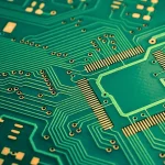
As the demand for faster, more reliable electronic devices grows, the role of High Frequency PCBs (Printed Circuit Boards) has become increasingly important. These specialized circuit boards are designed to handle signals at frequencies ranging from 500 MHz to several GHz, making them essential in applications such as telecommunications, radar systems, satellite communications, and advanced computing.
However, designing high-frequency PCBs comes with its own unique set of challenges. High-frequency signals are prone to loss, distortion, and interference, which can degrade the performance of electronic devices. To overcome these issues, PCB designers must address several key challenges while maintaining signal integrity, managing power consumption, and ensuring thermal stability.
In this article, we’ll explore the most common design challenges faced when developing High Frequency PCBs and discuss effective solutions to ensure optimal performance and reliability.
1. Signal Integrity and Loss
Challenge: Signal Integrity
Signal integrity refers to the quality of the electrical signal as it travels through the PCB. At high frequencies, even small deviations in the signal path can cause significant problems, such as signal degradation, distortion, or reflections.
High-frequency signals are sensitive to factors like trace width, via design, and material properties. These factors can lead to signal loss and signal reflections, which degrade performance and increase error rates. This becomes especially problematic in applications like 5G networks, radar systems, and satellite communications, where maintaining the integrity of the signal is crucial.
Solution: Controlled Impedance and High-Quality Materials
To address signal integrity challenges, one of the most important solutions is controlled impedance. Designers ensure that the PCB’s traces maintain a consistent impedance, typically 50 or 75 ohms, to minimize reflections and signal loss. Controlled impedance can be achieved by carefully adjusting trace width, spacing, and material thickness.
The material used for the PCB also plays a critical role in signal integrity. High-frequency PCBs often use specialized materials like Rogers or PTFE (Teflon) that have low dielectric loss and stable dielectric constants to maintain signal fidelity at high speeds.
Simulations using tools like ANSYS HFSS or Keysight ADS can help in predicting how the signal will behave, allowing designers to optimize the PCB layout and material choice for minimal signal degradation.
2. Electromagnetic Interference (EMI)
Challenge: EMI and Crosstalk
Electromagnetic interference (EMI) is a significant concern in high-frequency PCB designs. High-frequency signals can interfere with nearby circuits, leading to performance issues or even complete system failure. Additionally, crosstalk—unwanted coupling between adjacent traces or signal paths—can cause signal distortion and data corruption.
In high-frequency circuits, even the smallest trace or component can emit EMI, making it crucial to manage electromagnetic interference to avoid disrupting the operation of the PCB.
Solution: Grounding and Shielding Techniques
To minimize EMI, designers employ a variety of techniques:
- Ground planes: A continuous ground plane can help absorb EMI and provide a low-resistance return path for signals, reducing the chance of interference.
- Shielding: In some high-frequency designs, metallic shields are used to encase sensitive components or signal paths, preventing EMI from spreading.
- Differential routing: For high-speed signals, differential pairs are used to reduce EMI by ensuring that two signals, traveling in opposite directions, cancel out any interference.
- Trace separation: Adequate spacing between signal traces and between signal and ground traces can help prevent crosstalk and reduce the potential for signal interference.
Additionally, maintaining a tight stack-up with well-organized signal and ground layers in the PCB’s multilayer design helps improve shielding and reduces the chance of crosstalk and EMI.
3. Impedance Matching and Control
Challenge: Impedance Mismatch
Impedance control is one of the most critical factors in high-frequency PCB design. An impedance mismatch occurs when there is a discrepancy between the impedance of the transmission line (the trace) and the impedance of the components or connectors. This mismatch can lead to signal reflections, power loss, and decreased overall performance.
In high-frequency applications, such as RF and microwave circuits, maintaining a consistent impedance across the entire PCB is essential to ensure that signals travel without distortion or loss.
Solution: Precise Impedance Control
To solve impedance mismatch issues, PCB designers must maintain a consistent trace width and spacing in conjunction with the dielectric material. The thickness of the dielectric material and the trace width directly affect the characteristic impedance of a transmission line.
Using simulation tools like Impedance Calculators and 3D electromagnetic field solvers, designers can precisely determine the trace width, dielectric thickness, and stack-up structure needed to maintain the correct impedance. For high-frequency PCBs, this is particularly important to achieve 50-ohm or 75-ohm impedance, which is typically used for signal transmission.
Careful consideration of the via design is also necessary, as poorly designed vias can cause impedance discontinuities. Techniques like blind and buried vias, along with microvias, can help reduce impedance mismatches.
4. Thermal Management
Challenge: Heat Dissipation
High-frequency circuits generate heat due to the fast switching speeds of components. When signals travel through a PCB at high frequencies, power losses in the form of heat are inevitable. If this heat isn’t managed properly, it can lead to component failure, signal degradation, or even PCB warping.
As high-frequency circuits become more compact, heat dissipation becomes even more challenging. The inability to manage heat efficiently can result in thermal runaway, which can damage sensitive components and compromise system performance.
Solution: Advanced Cooling and Heat Management
To mitigate thermal issues, designers employ several techniques:
- Thermal vias: These are vias specifically designed to help transfer heat from the top layers of the PCB to the bottom or to heat sinks.
- Copper pours: Large copper areas in the PCB act as heat spreaders, dissipating heat more effectively.
- Active cooling: In high-power applications, such as RF amplifiers, active cooling solutions like fans or heat sinks can be used to draw heat away from the PCB.
- Material selection: Choosing materials with higher thermal conductivity helps dissipate heat more efficiently. For example, ceramic and aluminum-based PCBs can offer superior thermal management compared to traditional FR-4.
Designers also optimize the placement of heat-sensitive components and ensure that adequate ventilation is provided for the PCB.
5. Manufacturing Tolerances
Challenge: Tight Tolerances for High-Frequency Applications
High-frequency PCBs require very tight manufacturing tolerances, especially in the trace width, layer alignment, and hole sizes. Even a small deviation in the manufacturing process can cause significant performance issues, such as increased signal loss, impedance mismatches, or poor thermal dissipation.
For instance, trace width tolerances of just a few microns can make the difference between a well-functioning PCB and a failed one. As signal frequencies increase, the impact of manufacturing inaccuracies becomes more pronounced.
Solution: Precision Manufacturing and Advanced Tools
To meet these tight tolerances, manufacturers must use high-precision equipment and automated processes:
- Laser drilling for precise via placement
- High-precision etching for accurate trace width
- Advanced PCB stack-up techniques to ensure perfect alignment across multiple layers
Utilizing CAD tools like Altium Designer or Cadence Allegro allows designers to simulate manufacturing processes and account for any potential deviations before production begins. Additionally, working closely with an experienced PCB manufacturer ensures that the designs meet the stringent requirements for high-frequency applications.
Conclusion
Designing High Frequency PCBs presents a unique set of challenges, from signal integrity and EMI management to impedance control and thermal dissipation. Each challenge requires careful consideration of materials, design techniques, and manufacturing capabilities to ensure that the PCB performs optimally at high frequencies.
By understanding and addressing these challenges, PCB designers can create reliable, high-performance circuits that meet the demands of cutting-edge applications like 5G networks, aerospace systems, and advanced medical devices. With the right tools, materials, and techniques, designers can ensure that their High Frequency PCBs will function efficiently and consistently in the most demanding environments.


